Google+ VLSI QnA: truth table
Showing posts with label truth table. Show all posts

Sunday, 11 May 2014

D Flip flop

Q.1) What is D type flip-flop?


Answer) The D type flip-flop has one data input 'D' and a clock input. The circuit edge triggers on.the clock input. The flip-flop also has two outputs Q and not(Q). The operation of the D type flip-flop is as follows:
Any input appearing (present state) at the input D, will be produced at the output Q in next clock cycle
Example : If in the current time D = 0 and Q = 1, the next state will be D = (0/1) and Q = 0.

Truth table for D flip flop
Truth Table for D Flip Flop.

Q.2) Draw the excitation table for D - flip flop.


Answer) From the truth table, we can see that,
           When Q retains it state from '0' to '0' or changes from '1' to '0', the value of D is '0'.
           When Q retains it state from '1' to '1' or changes from '0' to '1' , the value of D is '1'.

Excitation table for D flip flop
Excitation table for D flip flop.

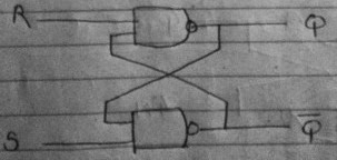
Q.3) Draw the circuit diagram of D - flip flop.

Answer) The circuit diagram for D flip flop can be easily drawn by converting the S-R flip flop into D flip flop. For converting one flip flop to another, a truth table is prepared by combining the excitation tables for both the flops. The given flop  (in this case S-R flip flop) acts as outputs and flop to be derived (in this case D flip flop) along with current output and next state output acts as inputs.


Combined truth table for converting SR flip flop into D flip flop
Combined truth table for converting S-R flip flop into D flip flop.

            K map for S simplification         K map for R simplification
K-Map Simplification

D flip flop using SR flip flop
D Flip Flop using S-R Flip Flop.

Q.4) Convert D flip flop into S-R flip flop.

Answer) In this case,
              Given flop : D flip flop (output)
              Flop to be derived : S-R flip flop (input)

Combined truth table for converting D flip flop into SR flip flop
Combined truth table for converting D flip flop into S-R flip flop.

K map simplification for D
K-Map Simplification


SR flip flop using D flip flop
S-R Flip Flop using D Flip Flop.

Wednesday, 7 May 2014

S-R latch and flip-flop

Q.1) Explain S-R Latch using NAND gates.

Answer) Latch is a sequential logic circuit which checks all its inputs continuously and will change its output as soon as the input changes without waiting for the clock signal. Generally an enable signal is provided for a latch. When the enable signal is active, the output will change as soon as there is change in input.

It has two outputs Q and not(Q) which are complements of each other.

The boolean equation for the outputs can be expressed as follows :
           Q = not(R.not(Q))
     not(Q) = not(S.Q)

I) S = 0, R = 0 (Race Condition)
    Substituting the value of S and R in the above equations, we get both Q and not(Q) as 1. This is an indeterminate state and should be avoided.

II) S = 0, R = 1 (Reset Condition)
     Since, S = 0, it forces not(Q) to be 1 and R = 1 forces Q  = 0.

III) S = 1, R = 0 (Set Condition)
       In this case, R = 0 forces the Q = 1 and S = 1 forces not(Q) = 0.

IV) S = 1, R = 1 (No change)
       Substituting the values of S and R in the above equation, we get,
       Q = Q and not(Q) = not(Q), hence there is no change in the outputs.

SR latch


SR latch truth table


Q.2) Explain positive edge triggered S-R flip flop.

Answer) The S-R flip flop consists of a differentiator circuit and a S-R gated latch. C-Racts  as a differentiator and converts the rectangular clock pulses into positive and negative spikes. The diode acts as a rectifying diode and allows only the positive spikes to pass through, blocking the negative spikes.

SR flip flop


SR flip flop waveform


SR flip flop truth table


Q.3) Draw the excitation table for S-R flip flop.

Answer) From the above truth table, we can infer following points :
  • When Q retains state '0',  we have two conditions S = R = '0' and S = '0'; R = '1', hence to retain state '1',     S = '0' and R = 'x'
  • When Q changes from 0' to '1', S = '1' ; R = '0'
  • When Q  changes from '1' to '0', S = '0' ; R = '1'.
  • When Q retains state '1' , we have two conditions S = R = '0' and S = '1'; R = '0', hence to retain state '1' ,     S='x' and R = '0'.
SR flip flop excitation table


Q.4) Explain race condition.

Answer) Race condition occurs when both S and R input of latch becomes '0'. When any one input to a NAND gate is '0',  its output becomes '1'. Thus both the outputs will try to become '1', hence it is called race condition.